As part of your design process, you'll need to start with a block diagram, circuit schematic, and eventually a PCB layout
Home
› Logic Diagram And Truth Table Of Sr : Flip Flops In Electronics T Flip Flop Sr Flip Flop Jk Flip Flop D Flip Flop Circuits : Please explain how the table evaluates the inputs.
Logic Diagram And Truth Table Of Sr : Flip Flops In Electronics T Flip Flop Sr Flip Flop Jk Flip Flop D Flip Flop Circuits : Please explain how the table evaluates the inputs.
Logic Diagram And Truth Table Of Sr : Flip Flops In Electronics T Flip Flop Sr Flip Flop Jk Flip Flop D Flip Flop Circuits : Please explain how the table evaluates the inputs.. Once the boolean expression is obtained as always we can build the circuit diagram using the or gates as shown below. Logic gates and truth tables. You'll not find this ebook anywhere online. A truth table is a device for using this form syntax in calculating the truth value of a larger formula given an interpretation (an assignment of truth values to sentence letters). A venn diagram is, in essence, a visual truth table.
It is seen from the fig that each gate has one or two binary inputs, a and b, and one binary output, c. At the most elementary level, an elecrtonic device can only recognise the presence or absence of current or voltage. Featuring a purple munster and a duck, and optionally showing intermediate results, it is one of the better instances of its kind. Da = x'y' + y'a db = y'b + xa z = b' (i) draw the logic diagram of the table. Flip flops input equations and the circuit output are as follows;
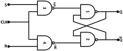
Flip Flops De Part 18 from www.engineersgarage.com Look at any books now and if you do not have a lot of time you just read, you are able to download any ebooks to your laptop and check later. At the end of the day, one of the few things, and. The small circles at the s and r input terminals represents that the circuit responds to active low input signals. A logic diagram uses the pictoral description of logic gates in combination to represent a logic expression. The user inputs the output values in the x column it will be a chart much like this Sr latch and sr flip flop truth tables and gates implementation. The symbol and truth table of a not gate with one input is shown below. I googled how the truth table functions for a while, but no luck to find a explanation.
At the most elementary level, an elecrtonic device can only recognise the presence or absence of current or voltage.
Block diagram, truth table, & logic diagram. I googled how the truth table functions for a while, but no luck to find a explanation. We will discuss each herein and demonstrate ways to convert between them. Representing data as binary values means. Once the boolean expression is obtained as always we can build the circuit diagram using the or gates as shown below. A venn diagram is, in essence, a visual truth table. Below shows the circuit symbol, boolean function, and truth. How to draw the logic diagram for this? Block diagram and gate level schematic of nand based sr latch is shown in the figure. Logic gate circuits are most frequently symbolized with a schematic diagram through their own exclusive symbols instead of their essential resistors and. When a logic gate has only two inputs, or the logic circuit to be analyzed has only one or two gates, it is fairly easy to remember how a. In the formal syntax, we earlier gave a formal semantics for sentential logic. The symbol and truth table of a not gate with one input is shown below.
Flip flops input equations and the circuit output are as follows; At the most elementary level, an elecrtonic device can only recognise the presence or absence of current or voltage. We will discuss each herein and demonstrate ways to convert between them. Da = x'y' + y'a db = y'b + xa z = b' (i) draw the logic diagram of the table. Construction of sr flip flop
T Flip Flop Toggle Flip Flop Circuit Nor Nand Working Applications from www.electronicshub.org Da = x'y' + y'a db = y'b + xa z = b' (i) draw the logic diagram of the table. Jk flip flop diagram truth tables explained. Logic diagrams and truth tables. Truth tables summarize how we combine two logical conditions based on and, or, and not. Featuring a purple munster and a duck, and optionally showing intermediate results, it is one of the better instances of its kind. Binary uses base 2, so we have just two possible values 1 or 0. For those who have a windows computer. There are a number of different logic gates that are each designed to perform a different operation in terms of output.
Truth tables offer a simple and easy to understand tool that can be used to determine the output of any logic gate or circuit for all input combinations.
Logic gate circuits are most frequently symbolized with a schematic diagram through their own exclusive symbols instead of their essential resistors and. The logic diagram consists of gates and symbols that can directly replace an expression in boolean arithmetic. Truth tables offer a simple and easy to understand tool that can be used to determine the output of any logic gate or circuit for all input combinations. Look at any books now and if you do not have a lot of time you just read, you are able to download any ebooks to your laptop and check later. An example below shows a logic diagram with. Construction of sr flip flop Creating a truth table involves a simple logic yet sometimes it may slow you down, especially when you are working on a last minute project. The logical diagram of the 3×8 line decoder is given below. Sr latch and sr flip flop truth tables and gates implementation. C3f8a logic diagram for t flip flop digital resources. 3 to 8 line decoder has a memory of 8 stages. It is seen from the fig that each gate has one or two binary inputs, a and b, and one binary output, c. You will learn how to construct truth tables for a number of combined logic functions.
Flip flops input equations and the circuit output are as follows; Representing data as binary values means. Construction of sr flip flop A venn diagram is, in essence, a visual truth table. An example below shows a logic diagram with.
The Gated S R Latch Multivibrators Electronics Textbook from www.allaboutcircuits.com The notation may vary depending on what industry you're engaged in, but the basic concepts are the same. Logic circuits are designed to perform a particular function, understanding the nature of that function requires a logic circuit truth table. Since we have thee outputs we will have three expressions as shown below. Look at any books now and if you do not have a lot of time you just read, you are able to download any ebooks to your laptop and check later. Binary uses base 2, so we have just two possible values 1 or 0. Does my truth table correct? It is seen from the fig that each gate has one or two binary inputs, a and b, and one binary output, c. Truth values in a computer :
Block diagram, truth table, & logic diagram.
Pls give truth table for gated sr. Electronics tutorial about sequential logic circuits and the sr flip flop including the nand gate sr flip flop switch debounce circuit. A = 0, b = 1, c = 1. At the end of the day, one of the few things, and. Each row will have different predetermined values as the truth table normally would have. A truth table is a device for using this form syntax in calculating the truth value of a larger formula given an interpretation (an assignment of truth values to sentence letters). Construction of sr flip flop Block diagram, truth table, & logic diagram. To study and verify the truth table of logic gates. Use the buttons below (or your keyboard) to enter a proposition. At the most elementary level, an elecrtonic device can only recognise the presence or absence of current or voltage. Truth table of nor based sr latch is given in table. Block diagram and gate level schematic of nand based sr latch is shown in the figure.